Applications of silicon-germanium heterostructures
This page gives an overview of our research in the field of silicon-germanium heterostructures. For further information, please see also our publications.
Applications of silicon-germanium heterostructures
-

SEM of an array of 8-µm tall Ge crystals grown epitaxially on Si pillars -
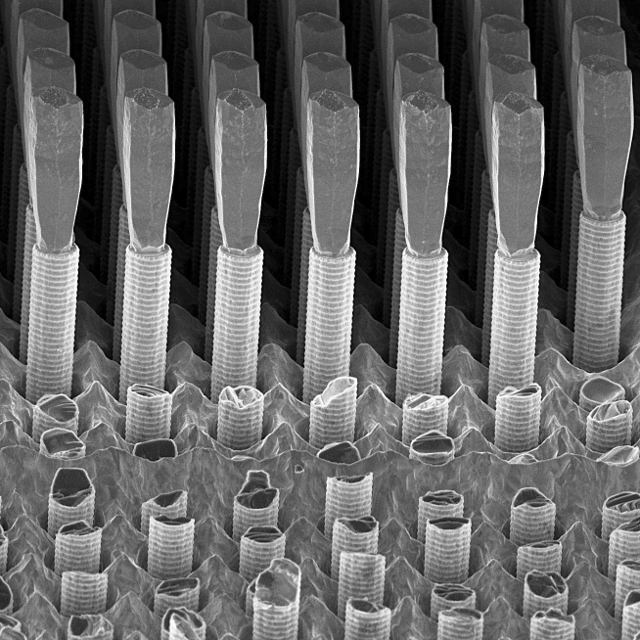
Array of etched, 8-µm tall Ge crystals grown epitaxially on Si pillars -

Infrared image taken with a Ge pixel detector integrated on a CMOS chip. Courtesy R. Kaufmann, CSEM Zürich -

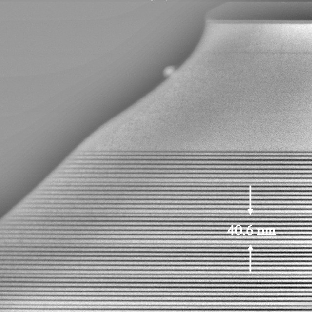
XTEM image of a SiGe quantum cascade structure. Courtesy E. Müller, EMEZ, ETHZ large_array Array of Ge crystals grown epitaxially on Si pillars. The array was obtained under conditions of self-limited lateral expansion of the crystals, thus preventing the latter to fuse and form a continuous film -

Array of Ge crystals grown epitaxially on Si pillars. The array was obtained under conditions of self-limited lateral expansion of the crystals, thus preventing the latter to fuse and form a continuous film

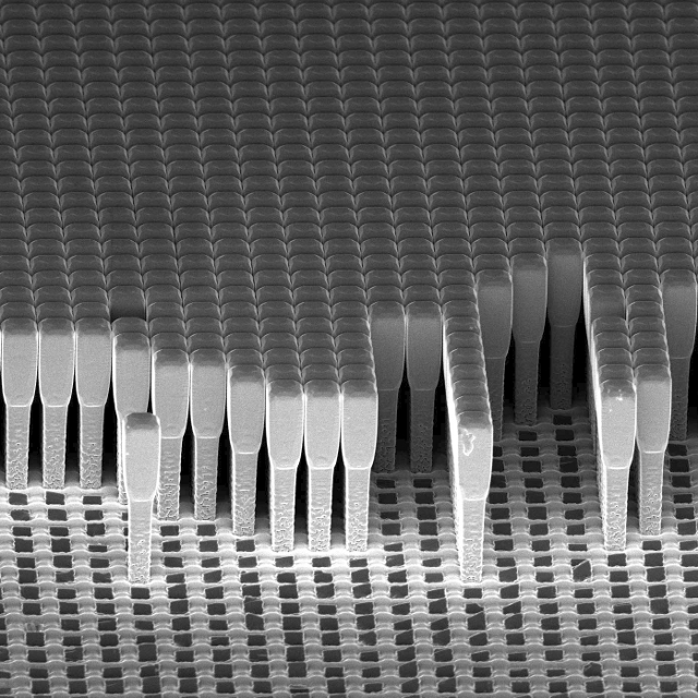
Our research is focused on the monolithic integration of dissimilar semiconductor materials with Si microelectronics for applications in the areas of X-ray imaging for medical applications, high efficiency multiple-junction solar cells and power electronic devices. For that purpose, we manufacture complex semiconductor systems consisting of virtually defect-free structures grown monolithically on cheap and abundant silicon substrates by epitaxial deposition techniques, such as low-energy plasma enhanced chemical vapor deposition (LEPECVD). Rather than being grown as continuous layers, these structures are composed of space-filling array of individual crystals, separated by narrow gaps of several tens of nanometers. In this way, crystal defects, normally present in layers of atoms differing in size, are entirely eliminated. Moreover, disruptive substrate bowing upon temperature changes, caused by unequal thermal expansion coefficients of dissimilar materials, is largely absent. Most importantly, fatal layer cracking induced by thermal stresses can no longer occur.
The structures are characterized by means of structural, electrical and optical tools, and optimized in close collaboration with groups from the Inter-University Center L-NESS (jointly run by the Politecnico di Milano and the Università di Milano Bicocca), and CSEM-SA.
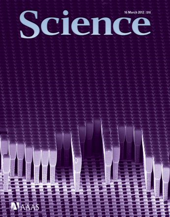
Article published in Science, featuring on the cover
Researchers from ETHZ and the CSEM Neuchatel, in collaboration with their Italian colleagues from the Politecnico di Milano and Università di Milano-Bicocca, have developed a novel method to manufacture highly perfect structures composed of different semiconductors to virtually any thicknesses on cheap and abundant silicon substrates. Instead of being assembled by state of the art bonding techniques the structures are grown in one piece, i.e. monolithically, by deposition techniques customary in semiconductor processing.